Analysis of the Tuggle Front End – Part II
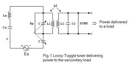
We shall now consider the Tuggle tuner
delivering power to a load. First, we must account for the parallel RF losses
of the unloaded tuned circuits. Let RP represent the losses of the tank
circuit comprising L1 and C, and RTNK those of L2
and C2 (please see Fig. 1).
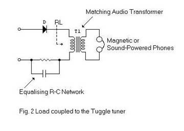
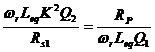
The load consists of a diode detector D in
series with an audio load RL (usually an audio transformer matching
a pair of 2k ohms DC resistance magnetic headphones or low-impedance sound
powered phones to the detector) and is coupled to the tuner via the magnetic
coupling existing between L1 and L2, being M the mutual
inductance of the coils. The secondary is tuned to the same radian frequency as
the primary. An schematic for the load can be seen in Fig. 2. Usually, it is assumed that optimum RF power
transfer occurs when the antenna-ground system resonance resistance r is
matched to the unloaded-secondary resonance parallel resistance RTNK,
with the diode detector´s input resistance matched to this combination. Thus, or This is the overall parallel RF resistance of
the secondary tank under matched conditions, and suggests that the unloaded Q
of this tank circuit has been reduced to ¼ of its value. In this case, the net parallel resistance to be
coupled to the primary is:
Some circuit equivalents
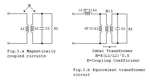
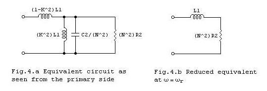
In Fig.1, let´s replace L1 and the
coupled secondary circuit by the equivalent shown in Fig.3.a, which in turn can
be replaced by the transformer circuit shown in Fig.3.b. In the transformer circuit, the impedance
coupled to the primary side consists of a capacitance C2 / N2
in parallel with a resistance N2R2. Both are in parallel
with the magnetizing inductance K2L1 (please see
Fig.4.a). K2L1 and C2 /
N2 resonate at a frequency
as The equivalent circuit of Fig.4.a reduces to
that of Fig.4.b, taking into account that for crystal set use, normally
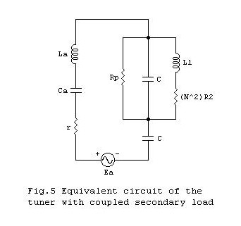
K<<1. Up to this point, in the tuner side we have the
equivalent circuit depicted in Fig.5. The series-coupled resistance N2R2
can be transformed into a resistance RP1 in parallel with RP.
Using the known series-to-parallel “loss resistance” transformation we get:
Let
Next, we compute the equivalent resistance RT
of the parallel combination of RP and RP1. It is given
by:
Substituting RP1 by its equivalent
given by eq.(3):
Letting
If
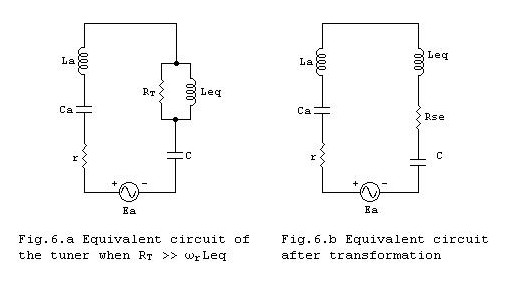
Applying a parallel-to-series transformation,
the equivalent circuit of Fig.6.b is obtained. The series transformed resistance Rse
is given by:
Let Rs is the series term due to RP
and Rs1, that coming from the coupled resistance N2R2.
Now, maximum RF power transfer to N2R2 occurs when:
or when: or From part I of this study we know that:
being
Then: Eq.(6) is now written as: Letting
Solving for K we obtain:
which gives the value of the coupling
coefficient for maximum RF power transfer to the secondary. Power calculationsThe RF power delivered to the secondary load of
Fig.1 will be at a maximum at resonance when eq.(6) is satisfied, this is, when
r + Rs = Rs1. The maximum available power is then:
where Ea is the peak value of the
voltage induced in the antenna. The power delivered to the secondary load R2
is the same as that dissipated by the coupled resistance N2R2.
To compute this power we need the voltage across L1 at resonance.
This is the same as the voltage across Leq in Fig.6.a. Then: From Fig.5 we obtain for the voltage across N2R2:
In crystal sets,
Bearing in mind eq.(3):
Substituting the value of ELeq given
by eq.(11) into the above expression we obtain: We can recall that:
Then:
Then, we obtain: The power dissipated by N2R2
is:
Eq.(12) can be written as follows:
or:
Substituting this equivalence into eq.(13): according to eq.(10). PMAX is then dissipated by N2R2
and by consequence, this power is delivered to the secondary load. Some experimental resultsTwo coils, L1 and L2,
were wound on 4.5” diameter styrene forms using 660/46 Litz wire. L1
measured 152 uH and L2, 222 uH. A two-gang 475 pF variable capacitor
with bakelite insulation was used to tune L1. L2 was
tuned with a 480 pF variable capacitor with ceramic insulators. Unloaded Qs for each of the tuned circuits were
measured at three frequencies. Accordingly, the corresponding RF losses were
calculated. Data is tabulated below.
C
: two-gang 475 pF variable capacitor with bakelite insulation C2 : 480 pF variable
capacitor with ceramic insulation Q2UL : unloaded Q of L2-C2
combination Q1, Q2 : defined in the text RP, RTNK: defined in the
text Using the tabulated data, values for the
optimum coupling coefficient K will be calculated for a working crystal set. f = 530 kHz L1 = 152 uH Ca = 200 pF (assumed) r = 30 ohms (assumed) A = 1.555 x 10⁵ ohms Q1Q2A = 2.938 x
1010 ohms K = 4.165 x
10-3 Check: f = 1
MHz L1 = 152 uH Ca = 200 pF (assumed) r = 30 ohms (assumed) A = 1.9 x 10⁵ ohms Q1Q2A =
2.334 x 10¹⁰ ohms K =
5.663 x 10⁻³ Check: f = 1.7
MHz L1 = 152 uH Ca = 200 pF
(assumed) r = 30 ohms (assumed) A = 4.068 x 10⁵ ohms Q1Q2A = 1.29 x
1010 ohms K = 8.324 x
10-3 Check: CommentsThe values obtained for the coupling
coefficient K hold for
Ramon
Vargas Patron Lima-Peru,
South America
April 1st 2004
|